
Electronic Devices and Circuits - Section 1 (6)
Electronic Devices and Circuits - Section 1
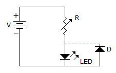
| 41. | In the circuit of figure the function of resistor R and diode D are
|
|||||||
Answer: Option C Explanation: Resistance limits current and diode is reverse connected and therefore protects LED against reverse breakdown. |
| 42. | Assertion (A): A p-n junction has high resistance in reverse direction. Reason (R): When a reverse bias is applied to p-n junction, the width of depletion layer increases. |
|||||||
Answer: Option A Explanation: The increase in reverse resistance is due to widening of depletion layer. |
| 43. | The amount of photoelectric emission current depends on |
|||||||
Answer: Option B Explanation: Only the intensity of incident radiation governs the amount of photoelectric emission. |
| 44. | In an n channel JFET, the gate is |
|||||||
Answer: Option B Explanation: Since channel is n type gate must be p type. |
| 45. |
|
|||||||
Answer: Option B Explanation: Emitter is p-type in p-n-p transistor. Therefore holes are majority carriers. |
| 46. | A transistor has a current gain of 0.99 in the CB mode. Its current gain in the CC mode is |
|||||||
|
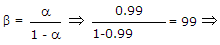 Current gain = 1 + β = 100.
| 47. | In which of these is reverse recovery time nearly zero? |
|||||||
Answer: Option C Explanation: In schottky diode there is no charge storage and hence almost zero reverse recovery time. |
| 48. | The most commonly used semiconductor material is |
|||||||
Answer: Option A Explanation: Germanium is rarely used. |