
Memory and Storage - General Questions (8)
Memory and Storage - General Questions
| 57. |
|
|||||||
Answer: Option B Explanation: No answer description available for this question. Let us discuss. |

| 58. |
|
|||||||
Answer: Option D Explanation: No answer description available for this question. Let us discuss. |
| 59. |
|
|||||||
Answer: Option D Explanation: No answer description available for this question. Let us discuss. |
| 60. |
|
|||||||
Answer: Option C Explanation: No answer description available for this question. Let us discuss. |
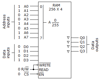
| 61. | The RAM circuit given below is suspected of being bad. A check with a logic probe shows pulse activity on all of the address lines and data inputs. The / line and inputs are forced HIGH and the data output lines are checked with the logic probe. Q0, Q2, and Q3 show a dim indication on the logic probe; Q1 indicates a HIGH level on the logic probe. What, if anything, is wrong with the circuit?
|
|||||||
Answer: Option B Explanation: No answer description available for this question. Let us discuss. |
| 62. |
|
|||||||
Answer: Option B Explanation: No answer description available for this question. Let us discuss. |
| 63. |
|
|||||||
Answer: Option C Explanation: No answer description available for this question. Let us discuss. |
| 64. |
|
|||||||
Answer: Option B Explanation: No answer description available for this question. Let us discuss. |