IndiaBIX
IndiaBIX
Start typing & press "Enter" or "ESC" to close
  • Home
  • Jobs
  • Results
  • Current Affairs
  • GK
  • Online Test
  • HR Interview
  • BLOG

Memory and Storage - General Questions (12)

  • Home
  • Electronics & Communication Engineering
  • Digital Electronics Questions with Answers
  • Memory and Storage - General Questions
Directions to Solve

Memory and Storage - General Questions

89. 

In a DRAM, what is the state of R/W during a read operation?

A. Low
B. High
C. Hi-Z
D. None of the above

Answer: Option B

Explanation:

No answer description available for this question. Let us discuss.

View Answer Discuss Workspace Report

90. 

The storage element for a static RAM is the ________.

A. diode
B. resistor
C. capacitor
D. flip-flop

Answer: Option D

Explanation:

No answer description available for this question. Let us discuss.

View Answer Discuss Workspace Report

91. 

What is the meaning of RAM, and what is its primary role?

A. Readily Available Memory; it is the first level of memory used by the computer in all of its operations.
B. Random Access Memory; it is memory that can be reached by any sub- system within a computer, and at any time.
C. Random Access Memory; it is the memory used for short-term temporary data storage within the computer.
D. Resettable Automatic Memory; it is memory that can be used and then automatically reset, or cleared, after being read from or written to.

Answer: Option C

Explanation:

No answer description available for this question. Let us discuss.

View Answer Discuss Workspace Report

92. 

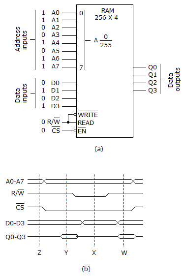
Refer to the given figures (a) and (b). A logic analyzer is used to check the circuit in figure (a) and displays the waveforms shown in figure (b). The actual analyzer display shows all four data outputs, Q0-Q3. The analyzer's cursor is placed at position X and all four of the data output lines show a LOW level output. What is wrong, if anything, with the circuit?

mcq12_1023_1

A. Nothing is wrong, according to the display. The outputs are in the open state and should show zero output voltage.
B. The circuit is in the READ mode and the outputs, Q0-Q3, should reflect the contents of the memory at that address. The chip is defective; replace the chip.
C. The circuit is in the mode and should be writing the contents of the selected address to Q0–Q3.
D. The Q0–Q3 lines can be either LOW or HIGH, since the chip is in the tristate mode in which case their level is unpredictable.

Answer: Option A

Explanation:

No answer description available for this question. Let us discuss.

View Answer Discuss Workspace Report

93. 

The check sum method of testing a ROM:

A. indicates if the data in more than one memory location is incorrect.
B. provides a means for locating and correcting data errors in specific memory locations.
C. allows data errors to be pinpointed to a specific memory location.
D. simply indicates that the contents of the ROM are incorrect.

Answer: Option D

Explanation:

No answer description available for this question. Let us discuss.

View Answer Discuss Workspace Report

94. 

How many address bits are needed to select all memory locations in the 2118 16K × 1 RAM?

A. 8
B. 10
C. 14
D. 16

Answer: Option C

Explanation:

No answer description available for this question. Let us discuss.

View Answer Discuss Workspace Report

  • 1
  • 2
  • 3
  • ..
  • ..
  • 10
  • 11
  • 12

Questions & Answers

Aptitude Chemical Engineering Civil Engineering Computer Science & Engineering Current Affairs Data Interpretation Electrical & Electronics Engineering Electronics & Communication Engineering General Knowledge Logical Reasoning Mechanical Engineering Non Verbal Reasoning Verbal Ability Verbal Reasoning

Interviews

HR Interview

Jobs

Sarkari Jobs

Results

Rojgar ResultSarkari Result

Admission

Admission 2023

Admit Card

Admit Card 2023

Answer Key

Answer Key 2023
copyright
Privacy Policy
© 2026 IndiaBIX. All Rights Reserved.

Report