
Field-Effect Transistors - General Questions
Field-Effect Transistors - General Questions
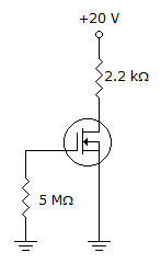
| 1. | Refer to the given figure. ID = 6 mA. Calculate the value of VDS.
|
|||||||
Answer: Option C Explanation: No answer description available for this question |
| 2. |
|
|||||||
Answer: Option D Explanation: No answer description available for this question |
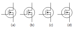
| 3. | Identify the n-channel E-MOSFET.
|
|||||||
Answer: Option C Explanation: No answer description available for this question. |
| 4. |
|
|||||||
Answer: Option D Explanation: No answer description available for this question |
| 5. |
|
|||||||
Answer: Option A Explanation: No answer description available for this question |
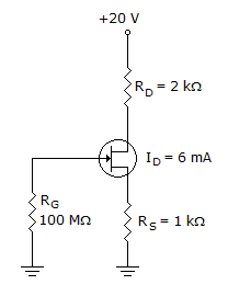
| 6. | Refer to figure shown below. What is the value of IG?
|
|||||||
Answer: Option D Explanation: No answer description available for this question. |
| 7. | Identify the p-channel E-MOSFET.
|
|||||||
Answer: Option D Explanation: No answer description available for this question. |
| 8. |
|
|||||||
Answer: Option C Explanation: No answer description available for this question |