IndiaBIX
IndiaBIX
Start typing & press "Enter" or "ESC" to close
  • Home
  • Jobs
  • Results
  • Current Affairs
  • GK
  • Online Test
  • HR Interview
  • BLOG

Programmable Logic Device - General Questions (3)

  • Home
  • Electronics & Communication Engineering
  • Digital Electronics Questions with Answers
  • Programmable Logic Device - General Questions
Directions to Solve

Programmable Logic Device - General Questions

17. 

GAL is an acronym for ________.

A. Generic Array Logic
B. General Array Logic
C. Giant Array Logic
D. Generic Analysis Logic

Answer: Option A

Explanation:

No answer description available for this question.

View Answer Discuss Workspace Report

18. 

What is the status of a tristate output buffer on a MAX7000S family device?

A. It is permanently enabled or disabled.
B. It is controlled by one of the two global output enable pins.
C. It is controlled by other inputs or functions generated by other macrocells.
D. All of the above

Answer: Option D

Explanation:

No answer description available for this question.

View Answer Discuss Workspace Report

19. 

Which of the following is true?

A. Altera uses PAL architecture and Xilinx uses PLA architecture.
B. Altera uses PLA architecture and Xilinx uses PAL architecture.
C. Altera and Xilinx both use PAL architecture.
D. Altera and Xilinx both use PLA architecture.

Answer: Option A

Explanation:

No answer description available for this question

View Answer Discuss Workspace Report

20. 

How many combinations are handled in an LUT?

A. 4
B. 8
C. 16
D. 32

Answer: Option C

Explanation:

No answer description available for this question

View Answer Discuss Workspace Report

21. 

FPGA is the acronym for ________.

A. Flexible Programming [of] Generic Assemblies
B. Field Programmable Generic Array
C. Field Programmable Gate Array
D. Field Programmer's Gate Assembly

Answer: Option C

Explanation:

No answer description available for this question.

View Answer Discuss Workspace Report

22. 

What does a dot mean when placed on a PLD circuit diagram?

A. A point that is programmable
B. A point that cannot change
C. An intersection of logic blocks
D. An input or output point

Answer: Option B

Explanation:

No answer description available for this question

View Answer Discuss Workspace Report

23. 

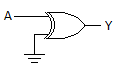
The output of this circuit is always ________.

mcq11_007

A. 1
B. 0
C. A
D. A

Answer: Option C

Explanation:

No answer description available for this question.

View Answer Discuss Workspace Report

24. 

What is the input/output pin configuration of the GAL22V10?

A. 10 output pins and 12 input pins
B. 2 special-purpose pins
C. 8 pins that are either inputs or outputs
D. All of the above

Answer: Option A

Explanation:

No answer description available for this question.

View Answer Discuss Workspace Report

  • 1
  • 2
  • 3
  • ..
  • 4
  • 5
  • ..
  • 7
  • 8
  • 9

Questions & Answers

Aptitude Chemical Engineering Civil Engineering Computer Science & Engineering Current Affairs Data Interpretation Electrical & Electronics Engineering Electronics & Communication Engineering General Knowledge Logical Reasoning Mechanical Engineering Non Verbal Reasoning Verbal Ability Verbal Reasoning

Interviews

HR Interview

Jobs

Sarkari Jobs

Results

Rojgar ResultSarkari Result

Admission

Admission 2023

Admit Card

Admit Card 2023

Answer Key

Answer Key 2023
copyright
Privacy Policy
© 2026 IndiaBIX. All Rights Reserved.

Report