
Transistor Bias Circuits - General Questions
Transistor Bias Circuits - General Questions
| 1. |
|
|||||||
Answer: Option D Explanation: No answer description available for this question |
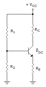
 DC result in changes in
| 2. | Refer to this figure. In the voltage-divider biased npn transistor circuit, if R1 opens, the transistor is
|
|||||
Answer: Option B Explanation: No answer description available for this question |
| 3. | Refer to this figure. Calculate the current I2.
|
|||||||
Answer: Option B Explanation: No answer description available for this question. |

 A
A
| 4. |
|
|||||||
Answer: Option D Explanation: No answer description available for this question. |
| 5. | Refer to this figure. The value of IC is
|
|||||||
Answer: Option C Explanation: No answer description available for this question |
| 6. |
|
|||||||
Answer: Option B Explanation: No answer description available for this question |
| 7. |
|
|||
Answer: Option B Explanation: No answer description available for this question |
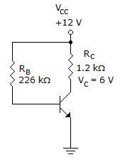
| 8. | Refer to this figure. Assume
|
|||||||
Answer: Option B Explanation: No answer description available for this question. |
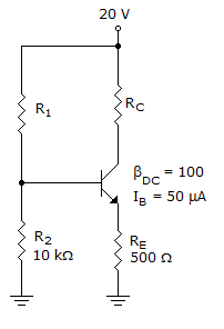 IC
IC  IE. Determine the value of RC that will allow VCE to equal 10 V.