
DC Biasing-BJTs - General Questions
DC Biasing-BJTs - General Questions
| 1. |
|
|||
Answer: Option A Explanation: No answer description available for this question. |
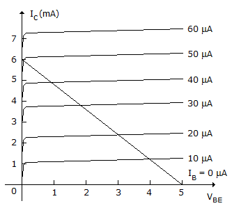
| 2. |
|
|||||||
Answer: Option D Explanation: No answer description available for this question. |
| 3. | Calculate VCE.
|
|||||||
Answer: Option B Explanation: No answer description available for this question. |

| 4. |
|
|||||||
Answer: Option C Explanation: No answer description available for this question. |


| 5. |
|
|||||||
Answer: Option D Explanation: No answer description available for this question |
| 6. |
|
|||||||
Answer: Option B Explanation: No answer description available for this question. |
 ?
?| 7. | Calculate Rsat if VCE = 0.3 V.
|
|||||||
Answer: Option A Explanation: No answer description available for this question. |

| 8. |
|
|||
Answer: Option A Explanation: No answer description available for this question. |