Describing Logic Circuits - General Questions (2)
Describing Logic Circuits - General Questions
| 9. |
|
|||||||
Answer: Option B Explanation: No answer description available for this question. Let us discuss. |
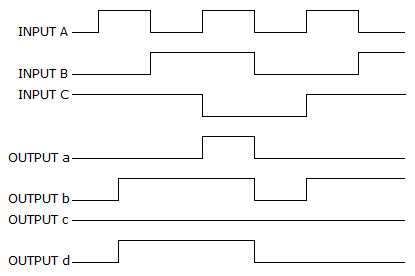
| 10. |
|
|||||||
Answer: Option C Explanation: No answer description available for this question. Let us discuss. |


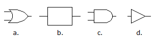
| 11. | Which of the figures given below represents an OR gate?
|
|||||||
Answer: Option A Explanation: No answer description available for this question. Let us discuss. |
| 12. |
|
|||||||
Answer: Option D Explanation: No answer description available for this question. Let us discuss. |
| 13. |
|
|||||||
Answer: Option D Explanation: No answer description available for this question. Let us discuss. |
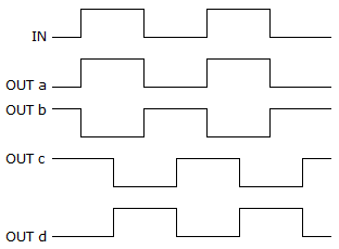
| 14. | Which timing diagram shown below is correct for an inverter?
|
|||||||
Answer: Option B Explanation: No answer description available for this question. Let us discuss. |
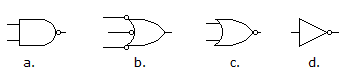
| 15. | Which of the figures given below represents a NAND gate?
|
|||||||
Answer: Option A Explanation: No answer description available for this question. Let us discuss. |
| 16. | For a 3-input NAND gate, with the input waveforms as shown below, which output waveform is correct?
|
|||||||
Answer: Option C Explanation: No answer description available for this question. Let us discuss. |