
Bipolar Junction Transistors - General Questions
Bipolar Junction Transistors - General Questions
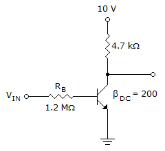
| 1. | Refer to this figure. Determine the minimum value of VIN from the following that will saturate this transistor.
|
|||||||
Answer: Option A Explanation: No answer description available for this question.
|
| 2. |
|
|||||||
Answer: Option D Explanation: No answer description available for this question.
|
| 3. |
|
|||||||
Answer: Option D Explanation: No answer description available for this question.
|
| 4. |
|
|||||||||
Answer: Option E Explanation: No answer description available for this question.
|
| 5. |
|
|||||||
Answer: Option D Explanation: No answer description available for this question.
|

| 6. |
|
|||||||
Answer: Option C Explanation: No answer description available for this question.
|
 A
A| 7. |
|
|||||||
Answer: Option B Explanation: No answer description available for this question.
|
| 8. |
|
|||||||
Answer: Option B Explanation: No answer description available for this question.
|